Nanomatťriaux : dťpŰts sous vide et rťalisation de foils mťtalliques
Introduction
The techniques of physical vapour deposition (PVD) covers a broad class of vacuum coating processes in which the material deposited is physically evaporated or sputtered from a source. These particles removed move in vacuum with a kinetic energy dependent on the method used, and just condense on the substrate to form a thin coating.
In the MMS Vacuum Unit located at “Pôle d’ingénierie des matériaux”, we have at our disposal a machine called EVA allowing to obtain thin metal layers and simple joining of materials (multilayers) ranging from the nanoscale the micrometer scale. Depending on the deposit material (pure metal, alloy, oxide, nitride) and target thickness, we can use 4 different techniques :
1. Cathodic magnetron sputtering
2. Self induced ion plating (SIP)
3. Depositionby electron beam (ebeam)
4. Jet vapor deposition (JVD)
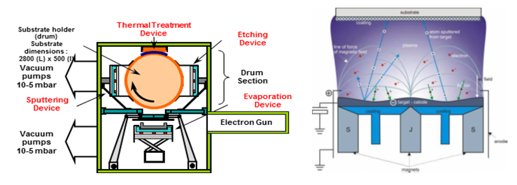
EVA device (sputtering, SIP, ebeam) sputtering
Each technology has its advantages and disadvantages and can be combined to obtain multilayers of different materials (combinations of pure metals, conductive layer/insulating ,barrier layers, reflecting layers of colored layers [oxides, nitrides], insulating layers [oxides] ...) with various thicknesses depending on desired applications. These techniques can be used to produce either foil or coating.
Foil manufacturing
The manufacture of thin sheets of metal used in fields ranging from electronics (Cu) to packaging (Al or Fe) is mainly realized by rolling and electroplating, which are energy-intensive processes and sources of chemical wastes. The vacuum deposition method enables the manufacture of metal foils in many different metals, while ensuring good quality of layers, the absence of any solid or liquid discharge and minimizing production costs.
Through these processes, it is possible to deposit metals (Zn, Cu, Ti, ...) on a substrate and thereby obtaining thin metal sheets by peeling the deposited layer. The thicknesses obtained ranged from a few microns to several hundred microns.
Through these processes, it is possible to deposit metals (Zn, Cu, Ti, ...) on a substrate and thereby obtaining thin metal sheets by peeling the deposited layer. The thicknesses obtained ranged from a few microns to several hundred microns.
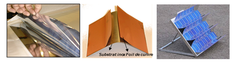
Zn foil – Cu foil for printed circuit boards – Ti reflector solar
Vacuum deposition
In addition to the foils, this technology allows to realize metallurgical coatings which have applications in diverse fields as:
- Mechanics : hard deposits TiN, coating nanoscale multilayer Ti-Al-N, nanocomposites ...
- Optics : low emissivity layer for building, anti-reflective layers, optical filter, self-cleaning glass, reflector, ...
- Electronics and energy : microbatteries Li, hearts of fuel cells, photovoltaic cells, ...
- Chemical industry : thin films having catalytic properties, ...
- Automotive sector : surface passivation, mirrors, ...
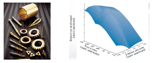
Applications example: hard deposits TiN (Titanium Nitride) on cutting tools
Nanomaterials
The obtained microstructures of the foils are relatively different from those obtained by rolling or electrolysis. These methods of vacuum deposition may lead to new materials: nanomaterials.
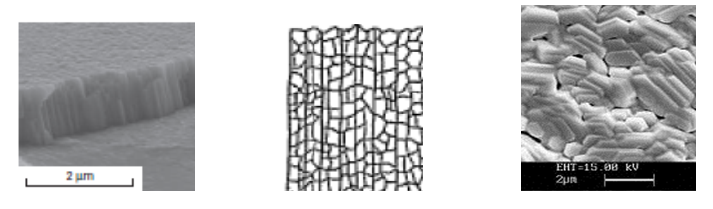 Microstructure : Isotropy of the grain orientation - no preferred direction
|
There is a high industrial interest for thin products (metallic foils and coatings of few microns to several tens of microns thick) made by vacuum deposition. This project consists of building a technology center to identify the needs of different partners in the creation of new materials (atom by atom), in order to create a launch pad for a project of greater magnitude with more mature products. The goal is to develop an innovative metallurgy: the nanometallurgy.
The unique properties of nanocrystalline materials result from their large number of grain boundaries compared to conventional polycrystalline materials. The structure of the interface plays an important role in the physical and mechanical properties of nanocrystalline materials. Nanocrystalline metals generally exhibit higher yield strengths and hardness compared to equivalent microcrystalline metals. Previous work indicates that these products are of great interest thanks to their special electrical and electromagnetic properties (dielectric, electromagnetic shielding ...).
Partnership ULg / ArcelorMittal / RW
Previous page: Matťriaux ŗ bas point de Curie
Next page: Caractťrisation des propriťtťs thermiques